
Koh Young
The Global Leader in True 3D Inspection
Solder Paste Inspection (SPI)
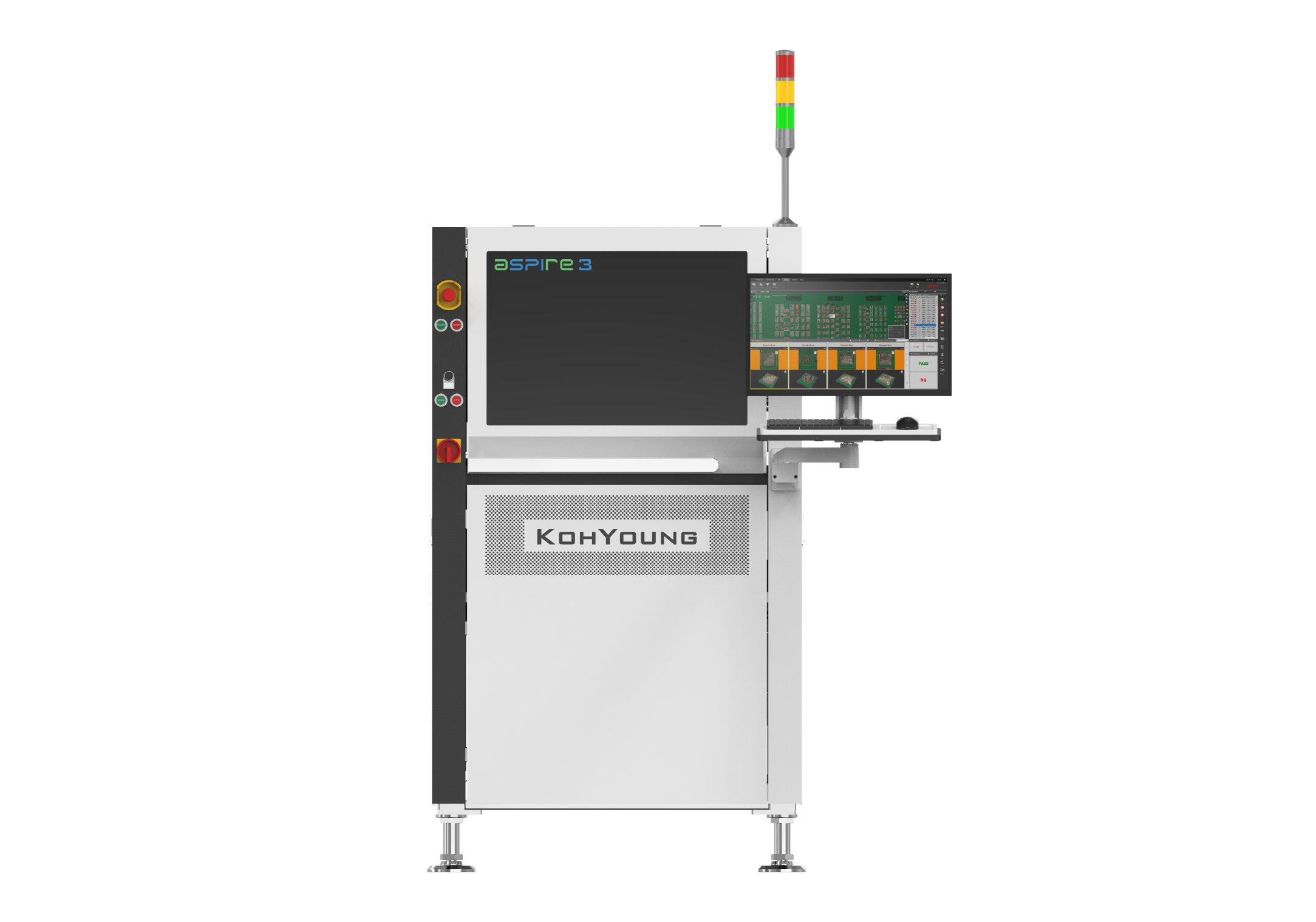
True 3D Insight Into Every Print
Since roughly 70% of SMT defects originate at the printing stage, catching problems early makes or breaks a line’s yield. Koh Young’s SPI systems measure the actual volume of every solder deposit — down to the smallest 03015 components — instead of estimating from a flat image.
Key Features:
- Shadow-Free 3D Measurement – Dual and quad projection eliminate the blind spots that trip up single-camera systems
- Active Warp Compensation – Automatically adjusts for board warpage so measurements stay accurate
- Auto-Rework Capability – Detects and corrects insufficient solder before it becomes a downstream defect
- Self-Diagnosis – Built-in predictive maintenance keeps the system running at peak accuracy
- Smart Factory Solutions – KPO Printer uses live SPI data to automatically fine-tune print parameters, keeping the printer running within spec without a dedicated process engineer watching over it
It’s inspection built to catch problems at the source, before they turn into scrap.
Automated Optical Inspection (AOI)
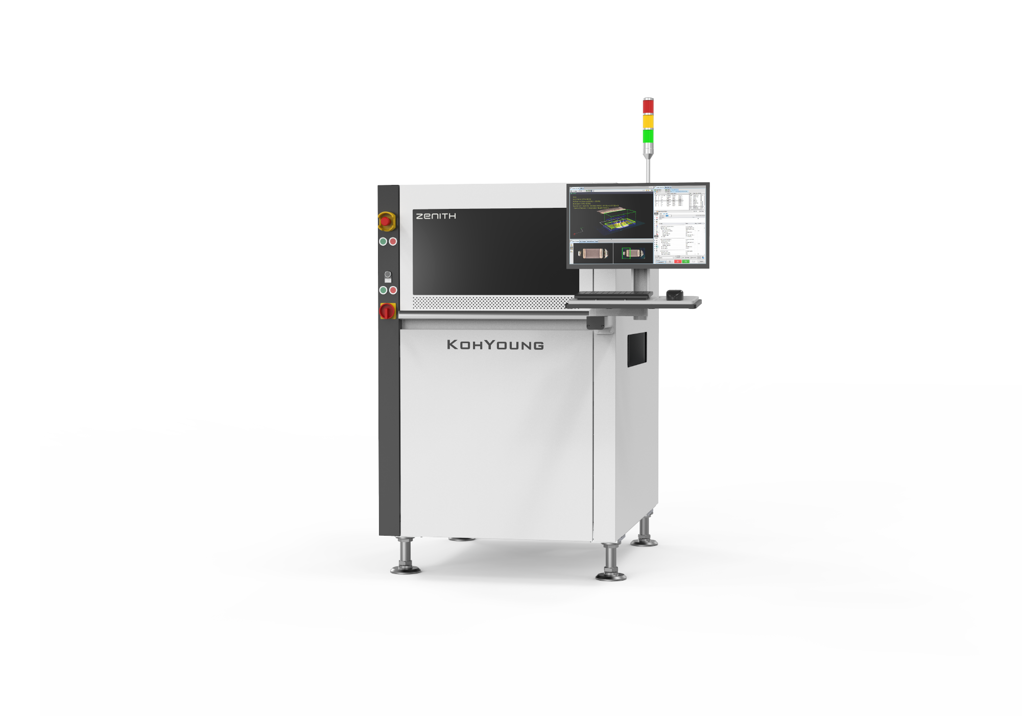
Seeing Every Joint the Way It Actually Looks
Conventional 2D and pseudo-3D AOI systems struggle with shiny components, shadows, and inconsistent lighting — leading to false calls and missed defects. Koh Young’s Zenith AOI line measures the true profilometric shape of every component and solder joint, delivering IPC-610-based results without a golden board or lengthy manual programming.
Key Features:
- True Profilometric 3D Measurement – Captures actual shape and height, not just a 2D silhouette
- IPC-610 Compliant – Built-in inspection standards eliminate manual threshold guesswork
- AI-Powered Auto-Programming – Cuts programming and production preparation time dramatically
- Side-View Camera Coverage – Extends inspection to leadless chips, connectors, and partially shielded components
- Smart Factory Solutions – KPO Mounter uses live AOI data to pinpoint the exact heads, nozzles, feeders, or components driving defects, then corrects mounting parameters in real time to keep the placement process on target
The result is fewer false calls, fewer escapes, and a lot less time spent second-guessing a defect.
Dispensing Process Inspection (DPI)
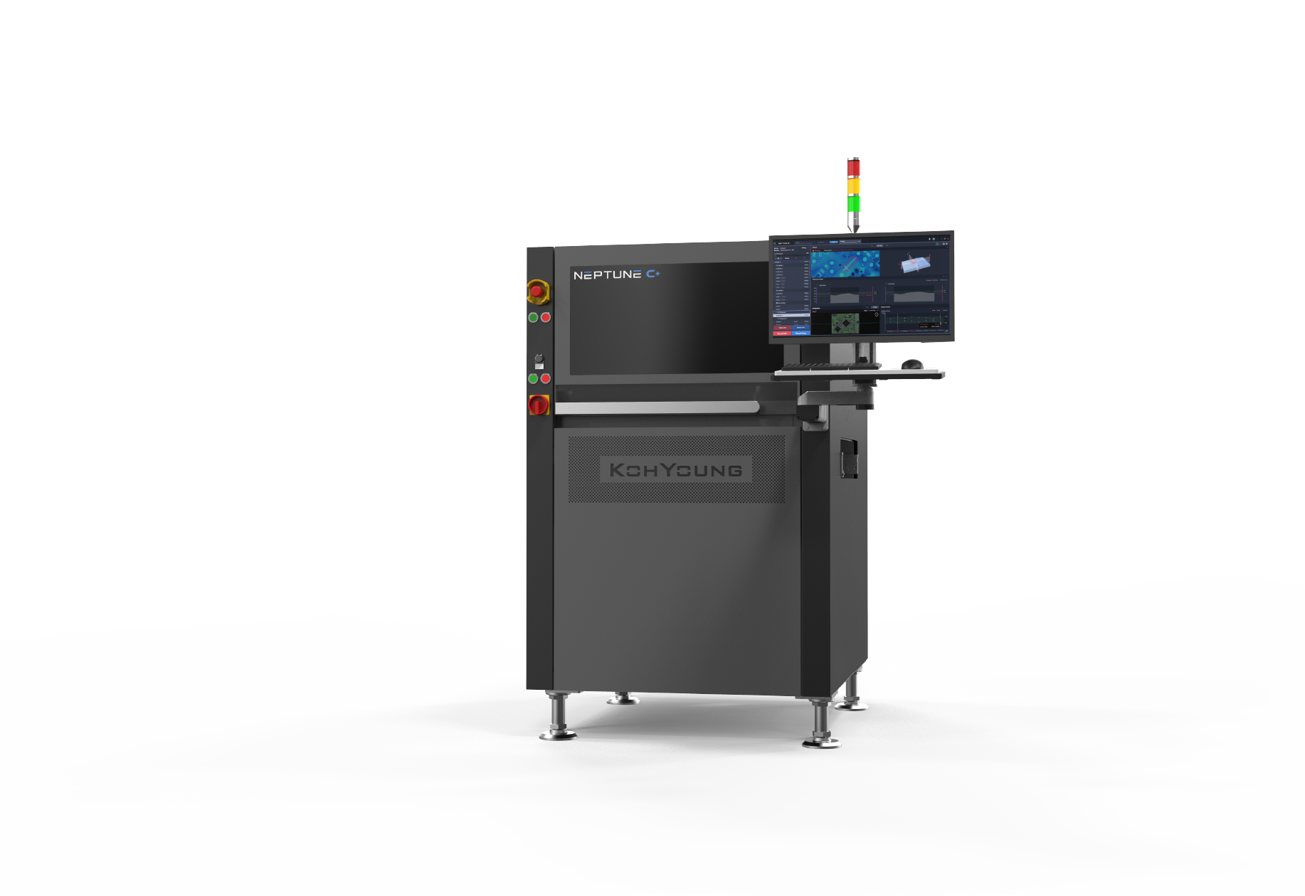
Full-Depth Visibility Into Coating & Dispensing
Conformal coating and dispensing processes protect a board from moisture, corrosion, and shock — but only if they’re applied correctly. Koh Young’s Neptune series sees through wet or dry material regardless of transparency, catching bubbles, thin spots, and coverage gaps that traditional UV-based systems miss entirely.
Key Features:
- Non-Destructive 3D Profiling – Measures thickness and coverage without damaging the material
- L.I.F.T. Technology – Sees through transparent, translucent, and pigmented coatings alike
- AI-Powered Bubble Detection – Identifies defects autonomously, without manual teaching or tuning
- Broad Material Compatibility – Handles acrylic, silicone, polyurethane, UV-cure, and hybrid coatings
- Top & Bottom Inspection – Covers both sides of a board in a single pass
It’s the kind of depth traditional optical inspection simply can’t reach.
Semiconductor Applications
Precision Inspection for Advanced Packaging
As components shrink and packaging gets denser, traditional inspection methods hit their limits — especially with mirror-finish dies and micro solder deposits. Koh Young’s Meister series combines advanced optics with Moiré-based 3D measurement to inspect what conventional systems simply can’t see.
Key Features:
- Reflective Component Inspection – Accurately measures mirror-surface dies where standard optical sensors fail
- Micro Deposit Accuracy – Captures ultra-fine, narrow-pitch solder deposits with confidence
- Advanced Packaging & Mini-LED Ready – Proven across hundreds of installed systems worldwide
- Flexible Substrate Handling – Supports diverse carriers, substrates, and vacuum chuck setups
- AI-Powered Defect Review – Auto-classifies defects and surfaces judgment history for faster decisions
With hundreds of systems already deployed globally, it’s inspection technology built for where packaging is headed next.
No Risk, No Stress, Only the Best.
PMR Representatives delivers superior products, materials and after sales support to give a better service and solutions to our customers.